

IC Substrates
An integrated circuit is any type of circuit made to fit onto a small chip. It can be a microcontroller, an amplifier or any other type of electronic component. The resulting device can be used to build complex projects such as GPS tracking devices, LED lights and automotive electronics. To create these advanced devices, a printed circuit board design is needed to connect all the chips together.
The IC substrate acts as the conduit for the PCB to the semiconductor chip, so it must be capable of handling high-density designs and precise manufacturing processes. In addition, achieving high yield in the manufacturing process requires that ic substrate manufacturers have the right equipment and robust quality control procedures to ensure consistent product performance and reliability.
IC substrates come in different classifications based on their package type, bonding technology and material attributes. Each classification can be further divided into different categories based on their specific application fields. Regardless of their differences, all IC substrates are crucial to modern electronic products, especially those that require advanced functions and thin, lightweight materials.
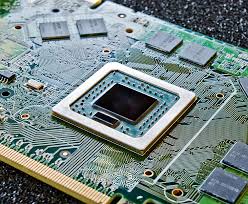
IC Substrates – All You Need to Know About Integrated Circuits
Rigid IC substrates are typically constructed using epoxy resin, BT resin or ABF resin. They are also characterized by their high thermal conductivity and low coefficient of thermal expansion (CTE). This type of IC substrate is most commonly used for mobile MEMS chip packaging, but it can also be applied to other products that need a rigid and durable carrier.
Semiconductor chips can have millions or even billions of components that need to be positioned and connected in a tight space. To do so, the IC substrate must be made of a rigid material that can support the weight and size of the chip while being flexible enough to allow for the construction of layers of insulating materials and conductive lines. The substrate must be thin enough to permit the use of very thin copper, but it must also be able to resist degradation and damage from the chemical processes involved in the fabrication and assembly of the IC.
To achieve high yield in the production of IC substrates, the manufacturer must implement rigorous quality control procedures to identify defects and remove them as soon as they occur. This is especially important when producing complex IC substrates with many different layers, as a single defect can ruin a large number of finished products. Fortunately, there are several tools available to streamline the entire manufacturing process and reduce the overall cost of an IC substrate.
The CAM and engineering software used in the manufacture of IC substrates can automate the analysis, optimization, imaging, inspection and panelization steps that are required for each job type. This allows for the efficient use of resources, reducing costs and improving efficiency. In addition, the flash etching and annealing techniques used in the production of IC substrates can also improve yield by ensuring that the final IC substrate has the desired circuitry pattern and function.