

microvias contribute to HDI PCB designs
As part of high density interconnect pcb, microvias are essential to keeping up with the increasing demands on PCB designers for finer I/O pitch and shorter signal transmission. They make it possible to pack more components into a dense board by allowing the use of smaller traces that improve signal performance and reduce crosstalk between layers. They also help reduce power consumption by reducing the distance electrical signals have to travel, and they contribute to lower manufacturing costs by decreasing the amount of material required for circuit board fabrication.
While presenting some fabrication difficulties for less-advanced manufacturers, microvias are indispensable to high density interconnect pcb technology. They are primarily responsible for saving space in these dense boards by making connections between layers, allowing more components to be packed into a single board, while also lowering costs. In addition, they make it possible to use smaller resonant circuits, and provide more flexibility for routing in these highly complex boards.
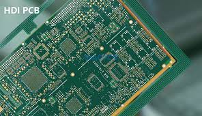
When via holes reach the limits of what can be mechanically drilled, an alternative process is required to form the interconnects between layers. Microvias are used to solve this problem by forming low aspect ratio holes that are not visible on the surface of the board. These microvias can be stacked or staggered, and they may be filled or unfilled.
How do microvias contribute to HDI PCB designs?
Fillered microvias are usually made of pure copper or an epoxy + copper resin, and they are plated with a conformal or pulse plating process. In the case of a conformal plating process, the use of additives in the filler material is important to prevent void formation. This is because the copper will tend to concentrate along the walls and top surface of the microvia if the plating process does not include these additives.
Stacked microvias are stacks of buried vias that are placed one on top of another, and this is the standard way to span between multiple layers in an HDI PCB. In contrast, staggered microvias are offset from one another and can be used to spread layer transitions out in the plane for components or traces that may not fit within the desired drilling zone.
As long as the PCB is properly designed and manufactured, these interconnects should be very reliable. Appropriate material selection, adherence to IPC-T-50M guidelines, and consistent resistance monitoring during reflow play a critical role in improving the reliability of microvias, as well as preventing latent failure modes from being triggered by thermal excursions during reflow.
Another benefit of using microvias is that they can save space by avoiding the need to place a ground plane between the component and the board. Instead, these buried or blind vias can be connected to each other by a short trace section that comes off the pad and makes contact with the microvia at its center point. This method is especially useful in resonant circuits to minimize the inductance of the primary and secondary resonant elements and to reduce the phase shift between them.