

Back Drilling Be Automated in PCB Fabrication Processes
Back drilling is a PCB fabrication process that removes the unused portion of through-hole vias. It is a vital step to minimize signal reflections and impedance discontinuities, especially in high-speed designs. Via stubs are a major contributor to signal reflections, affecting signal integrity and performance. By reducing the stub length through back drilling, you can minimize signal reflections, improve EMI immunity, and increase the frequency range of your signal. This will allow your design to operate at higher speeds with better accuracy and reliability.
Back drilling also prevents the creation of unnecessary copper plating on the back of the PCB, avoiding extra cost and reducing the overall thickness of the board. It’s important to work closely with your PCB manufacturer to ensure they understand your design requirements and manufacturing capabilities.
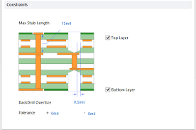
In order to back drill, you must first enable the feature in your tool’s software. This can be done by selecting “Back drilling” in the Layer Stack Manager mode and then entering the desired first and last layer thicknesses. The tool will then calculate the required drill depth to back drill through all layers between these values. The tool will then display the resulting back-drilled hole size in the Back Drill Layers panel.
Can Back Drilling Be Automated in PCB Fabrication Processes?
After you back drill, you must clean and inspect your circuit board to remove any debris or burrs. You can use a vision system or alignment tools to verify the location of the back drilled holes and ensure they are positioned correctly. You can also use automated optical inspection (AOI) to check the back drilled holes for any defects or deviations from your design specifications.
To get the best results, it’s recommended that you choose a back drill hole size slightly bigger than the original through-hole via. This allows the unused portion of the via to be removed without damaging other planes in the circuit board or the surrounding signal traces.
It’s also important to keep in mind that back drilling is a time-consuming and expensive process, so it’s best to avoid it if possible. Instead, you can consider using buried and blind vias for low-speed signals, or implementing controlled impedance routing on high-speed signal lines.
The main purpose of back drilling is to reduce the number of via stubs and the resulting signal reflections, which are common causes of poor signal integrity in high-speed PCBs. This technique can be a valuable tool for high-speed design and fabrication, but it is not foolproof. Therefore, it’s best to work with a trusted PCB manufacturer and consult a back drilling expert to ensure your boards will be produced to the highest standards.
In addition, it’s important to consider the layout of your high-speed circuits and optimize their performance by incorporating signal integrity improvements into the design. This includes minimizing via stub length, using buried and blind vias where applicable, and collaborating with your manufacturers to implement the best back-drilling practices for your specific project. By following these tips, you can avoid costly mistakes and achieve a high-performance PCB that complies with industry standards.